Weir PW
Precise Process Behavioral Models for OPC Photomask Feature Optimization

View Portable Document Format (PDF)
See Also: Weir PW Brochure
Other tutorials in the user's section: White Paper Tutorials
Contact TEA Systems for a Weir Demonstration or Logon
A new feature for version Weir PW ver: 4.3
Precise OPC and Phase Shift Reticle Qualifaction
Abstract
Describes the function and tools available for the comparative analysis of individual photomask features and modeling of their performance and robustness to semiconductor process variations for multiple Optical Proximity Correction (OPC) designs and neighbor environments on a photomask.
The Weir PW OPC extraction tools provide an additional benefit of improved accuracy and speed during simulation software calibration to the target process. Greater accuracy is achieved using proprietary modeled deconvolution methods and a comparative approach to derive true feature design response to process and tool perturbations. The precision of the analysis is greatly enhanced by the unique methods employed in the software to intelligently identify and remove soft metrology errors and discover the feature’s true response using Weir PWs inherent proprietary adaptive modeling techniques.
Keywords: DoF, Focus, Depth of Focus, Uniformity, IFD, process setup, metrology, model, Locus of Focus, LoF, Effective Dose, Exposure-Dose, lithography cell, HTML Reporting
Objectives
Application Objectives
Provide highly automated analyses of OPC feature response to tool and process variation.
Deliver unequaled precision in the calculation of individual OPC structure response for simulator setup.
Provide comparative tools for similar OPC structures during the layout and simulation phase of reticle design.
Characterize individual OPC structure response to variations in optical train perturbations.
Discriminate between pure errors and the systematic contributions of the process and tools.
Substrate and film response model mapping.
Provide a software toolset for the calculation of optimum focus and exposure-dose of semiconductor device reticles with the added determination of full-field and process contributed variation.
Supply advanced visualization tools for data and performance using advanced coupling of graphics and data plots.
Sections
Description of Weir PW OPC Extraction
Need in the Industry
Weir PW provides a suite of tools for photolithographic process setup and qualification using unique methods for metrology characterization, variable covariance analysis, precision calculation plus multi-site & feature process window calculation. Additional tools in the program provide an advanced and unique capability for wafer, field and sub-field (slit & scan) spatial modeling of feature and film perturbations.
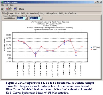
Optical Phase Correction (OPC) elements as well as any photomask atomic when printing features sizes less than 90 nm are employed provide a unique challenge to designers as shown in Figure 1. For many years Lithographers have realized that the high-frequency elements of features, such as corners and sub-wavelength outriggers, support fine structure that resides below the resolution of the lens. While these features could not be precisely resolved they still react strongly as wavefront perturbation sources and therefore exert a strong influence on the fidelity of the final image. This influence extends well beyond the immediate vicinity of the element by the wavefront perturbations of flair, scatter and distortion. A distortion that can influence and degrade the imaging of neighboring structures as far away as several microns.
Production Image Degradation
The imaging performance of the “lens” of an exposure tool is strongly influenced by the proper setup of the entire optical train. Drift or improper balance of the source, condensing optics, baffles and pupils degrades optimal imaging performance. The photomask when inserted into this optical train becomes an integral element in the imaging quality of the exposure tool.
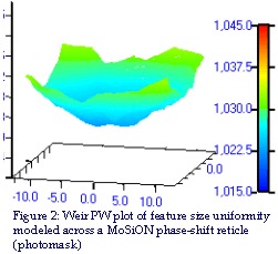
Ironically the photomask, which defines the object to be imaged into the photoresist, has long been known as a major source of image degradation. The photomask is a complex optical element that consists of a thick, typically quartz substrate upon which Chromium or other opaque or sometimes translucent film is patterned to construct the imaging object of the exposure tool. In addition to the anticipated manufacturing problems, such as uniformity such as shown in figure 2, the mask-element acts as vary dynamic optical element of the exposure tool. The photomask induces both refractive behavior and knife-edge scattering at the edges of the pattern. Recent OPC techniques further complicate the interactions through the use of phase, polarization and pellicle protective technology.
Even early applications were concerned with tilt, bow and flatness of the photomask. Wear and tear on the kinematic support structure was one of the earliest recognized contributors to image distortions. The photomask introduces a dynamic element to the production cycles since it is a lens element that is frequently changed in the production cycle. Production handling of the mask introduces patterning problems from sources such as feature edge erosion, film deposition and electrostatic discharge across its surface.
The incessant migration of the semiconductor imaging technology to the lower actinic wavelengths of current production coupled with the introduction of large stresses introduced by the mechanical scanning elements of a lens-slit aperture further increases the number of production sources of degradation and exposure tool-to-tool variability in image quality. These sources must be monitored if severe excursions of the production cycle are to be avoided.
Wavefront Engineering Consideration of the Photomask
Photomasks are evolving from the simple binary images of a few short years ago. Sub-wavelength imaging concepts provide opportunities for feature localized wavefront control to extend resolution and structure-selective depth-of-focus to regions unanticipated even a decade ago. The most publicized of these engineered wavefront perturbations include localized phase-shifting of critical features, sub-resolution scatter-control elements and inverse lithography systems that derive mask-feature patterns by an inverse convolution of the perturbations of the lens with the desired design circuit image on the wafer.
The most critical device levels that employ these methods therefore pose the problem that what-you-see on the photomask is not what-you-get on the final-image in the photoresist. The fact that the current state of technology for today’s simulators used in the design of these non-intuitive structures assumes stable and ideal lens performance characteristics. Process film interactions and interactions of the lens and photomask structure are significant complications ignored during simulation. Additional optical artifacts such as the obscuration that occurs near the exposure field extremities, lens flare, haze, effective polarization, coherence and numeric aperture are also not accounted for. These aberrations interact with feature-density lens heating and illumination drift to dynamically change image quality from exposure tool-to-tool and over time. The dynamic nature of these interactions are too facility specific and complex to be anticipated by any simulation.
Sub-resolution imaging is also sensitive to the characteristics and stability of the substrate. The photoresist is just one element that resides in a stack of translucent films present on the semiconductor wafer. Variations caused by bake-plate uniformity, developer deposition, true focus of the image, anti-reflective coating characteristics and the individual chemicals and tools that make up the lithograph-cell’s unique signature all contribute to variations that must be considered in the calibration of the simulator.

Another characteristic ignored by all simulators is the varying response of the image profile in the wafer film-stack to the process variations just discussed. Profiles change their response signature with location in the image field of the lens or through the frequency-domain of the exit pupil. Weir’s ability to measure the individual response signatures of the full profile and film stack provides the opportunity to comparatively select the best designs from actual performance data, see Figure 3.
The Weir PW analysis plot of figure 3 contains highly significant information about the OPC structure response and the health of the exposure toolset used in the analysis. The SWA variable curve of figure 3 shows the response of the offset or “Piston” coefficient of the model with error bars for each values standard derivation of the residuals to this coefficient.
The “Mean” variable plot shows the average value of all systematic field values to the process exposure variations with error bars for the Standard Error of the Mean (SEM) associated with this average. This curve therefore details the process and tool response of the OPC family without metrology soft errors and process random errors.
A large difference between the Piston and Mean curve values indicates significant aberrations associated with the exposure tool imaging.
Simulators properly calibrated to the unique characteristics of a tool-set and it’s interactions with the facility specific process will be able to properly compensate not only for variations across the process window but also those associated with the film stack and toolset.
Needed Refinement of the Raw Metrology Data
Effective simulator calibrations require the precise response characterization of individual feature atomics. The very nature of the active mask element and its dynamic interactions with the imaging system dictate that reticle feature design optimizations are a strong function of the target process. Small changes in feature structure can respond very differently depending upon the target process, the toolset and their unique response to feature size, orientation and location in the exposure field.
Accurate metrology must incorporate the response of full filmstack profiles to accurately characterize the performance of the target process as its behavior varies across the exposure field extremities during daily process variations. The elements of profile and film metrology by themselves contain too much noise to effectively discriminate between the inherent random and systematic perturbations introduced by the exposure and metrology tools. Pure statistical analyses can be not only inaccurate but also misleading.
Soft metrology errors introduce a more sinister component to the raw data. These errors represent metrology errors that are not blatantly deviant and only differ from the true feature value by a few percent. Target acquisition errors of the metrology tool similar to those shown in figure 4, substrate charge buildup in Scanning Electron Microscope metrology and even environmental perturbations such as short vibration occurrences contribute strongly. Target acquisition errors do not always result in aborted measurements but more frequently result in the measurement of a similar neighboring structure on the current or previous lithography level. Soft errors can even be operator contributed, appearing during creation of the metrology recipe.
Accurate photolithographic OPC feature characterization requires the raw data to be simultaneously modeled for systematic process and exposure errors. Adaptive modeling with the ability to include only statistically significant perturbation response must be employed. Inherent in these advanced modeling techniques must also be automated methods of aberrant datum singularity removal that otherwise would bias feature behavior signature extraction.
Product Scope
Weir PW’s OPC characterization software suite provides value in both engineering and production applications. Users working in the photomask, semiconductor, yield and design segments of the semiconductor industry can benefit from the analysis to both improve the design-for-manufacture sequence and monitor the stability of daily production.
The Weir PWTM product incorporates a suite of tools for the analysis, control and setup of the semiconductor lithographic process. Each module can be used separately or in conjunction with others, sharing a common interface, design and feel. Weir PW provides the most accurate analysis in the industry because of its ability to incorporate and differentiate the contributions of all sources of image perturbation.
The suite applies proprietary in-house developed “smart” modeling tools that recursively adapt to the data population and systematic components of the analysis. The results of smart modeling are realized through the improvements in the accuracy of derivation of production control surfaces that eliminate process correction ringing and run-off. Both control and analytical functions are accuracy enhanced by the product’s ability to include automated and manual culling of poor metrology. A library of process, process window, exposure tool and metrology models are included for systematic response extraction of tool and process variables from the metrology.
Weir PW provides an open system of access and versatility. Any form of metrology data can be easily imported into Weir PW. Data is stored in Microsoft ExcelTM worksheets for easy access and customization. Weir PW is capable of importing any format of commercial data. This support is extended free of charge to users with current warranty or maintenance agreements.
Multiple levels of data culling and range selection are available. Automated culling extracts metrology errors based upon range and sub-population distribution relative to a population median. This culling can be applied to raw data visualization or as an integral part of the model-application process. The limits for coefficient inclusion are dynamically adjusted based upon the uncertainty of each elements estimation and the number of data points in the data-surface.
Data can also be excluded interactively during graphic display using mouse-selection by data point, field site and wafer. The pain involved in manual sorting and exclusion of individual data points using text editors or spreadsheet tools is entirely eliminated.
Weir OPC Extraction uniquely applied these tools to the individual feature on the reticle based upon their feature-family designation as assigned by the user or metrology recipe. The models can be applied to any metrology including film thickness, feature widths, profile slopes and foot-size as well as temperature and trench depths.
The Customer
The Weir PW OPC extraction is a valuable tool for photomask, device design and semiconductor process engineers.
Photomask engineers can benefit from the tools ability to be used on both mask-facility as well as semiconductor gathered data. The software is capable of importing reticle metrology and storing the data into a reticle library for later use with wafer-gathered information. Weir PW can also be used to confirm final feature image uniformity and provides the ability to discriminate between photomask and semiconductor process and exposure tool systematic errors.
Reticle design engineers benefit from Weir PW’s automated yet highly interactive tools for the deconvolution of random and systematic errors introduced by the process and exposure toolset. Of particular importance is the ability of Weir PW to comparatively evaluate the response of individual OPC structures to these perturbations. Weir PW therefore provides a tool for determining the best resolution enhancement technique on a basis of both optimum exposure performance and the technique’s robustness in the presence of the perturbations introduced during production.
OPC Performance data is derived from systematic models that characterize the response of each feature using metrology actually taken from the production wafer. The user is therefore provided with the precise knowledge of the response characteristics of each structure’s sensitivity to exposure tool compared to process variation as well as the level of precision contributed by the metrology.
Description of Weir PW OPC
Extraction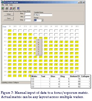
Supporting Functions
Data import from any industry standard metrology vendor format.
An open data storage format.
Data conversion into a Weir PW standard format spreadsheets for storage or use by other programs.
Tools for specifying setup, scan, exposure and focus layout of the raw data focus-exposure matrix.
Graphic interface for manual insertion of additional data into focus-exposure matrix data, Figure 5. This tools is often used for observation inclusion such as SEM studies of the number of nested elements still standing in a given exposure of dense–packed lines or via classification. Values entered can then be used as analysis elements or as a basis for culling.
Tools for manual specification of critical feature target and threshold size.
OPC Family Structure
Metrology tools often concentrate on the measurement of specific features of the
photoresist profile. Data sets include multiple measurements of a single
structure such as the “Bottom”, “Top” and sidewall angle (“SWA”) or profile edge
slope.
OPC structure studies however can include multiple design methods to achieve target feature sizes. For example sub-resolution outriggers may be designed with varying length, width or at multiple distances from the device feature. Phase-shift techniques also present multiple choices for the designer that can incorporate adjustments such as the size of the shifting structure or its phase-depth. Sometimes an exact quarter-wave shift is not the optimum construct because of interactions with the full-optical train of the exposure. Often several structures are capable of achieving the target size under optimum exposure conditions yet will exhibit varying levels of tolerance to variations in process and exposure during production. Similarly, the structure optimizations obtained at field center will not be optimized for structures located at other locations in the exposure field.
A number of metrology tools allow the feature target design names to be specified as part of the tool recipe. Multiple targets are measured in the same dataset for structures with varying layout configurations such as neighbor distance, orientation and density. Weir PW automatically sorts these targets and designates each using the “Sites” spreadsheet specifying each target family and it’s location on the exposure filed as shown in figure 6.
During an analysis the user can selectively analyze any single target in the data or any combination of target subsets using a simple family selection interface checkbox array. If multiple families are selected, the Weir PW analysis then repeats it’s analysis for each family as a separate sub-population of the data. Results are summarized in spreadsheets inserted into the data workbook and by using graphic comparisons.
Metrology tools that support this type of automated family designation in their output files include Scanning Electron Microscopes (CD-SEMs) such as the Hitachi, Applied Materials and some KLA-Tencor generations.
Scatter and ellipsometry metrology tools for the most part do not include family designations. Target performance evaluation data will include several datasets restricting data of one target family to each dataset. Weir PW can easily combine data in this format by first importing it into the Weir standard spreadsheet and then combining the multiple datasets by cutting and pasting the Data and Sites datasheets using the powerful capabilities of the Excel interface.
User Interface
Weir PW supports a full Graphic User Interface that interacts with the Microsoft Excel program for the storage of both the data and reports generated by the various analysis functions. Data is loaded into a proprietary Lot-Object that provides lot-wafer-field-site-measurement linked drill-down generation of graphics, data culling, display and charts.
Graphic captures are easily conducting using the mouse or menu-driven commands. Data sub-sets can be displayed by boxing in the area of interest to select observation of the data values or detailed plots or response in the area.
OPC Family Analysis
Note that this is the engineering interface of Weir PW. These analyses can be automated and trendcharted using Weir Macro’s and the Weir DM or Weir DMA software.
Start the Weir PW interface by selecting the menu shortcut or any of the installed shortcuts on your desktop or windows Launch Bar. The Data Selection interface shown in figure 7 will appear.
Data is be loaded into the interface by using the File/Open menu or by dragging a file onto the graphic display window. New metrology files or previously imported Weir Spreadsheet data files can also be loaded.
The site locations on the field are shown in the graphic display on the lower left. Wafer data is displayed to the lower right.
Controls at the top of the screen list the wafers of the lot, the exposure-dose values present in the data, scan-direction etc. Three drop-down controls are located at the top of the interface to allow selection of the variable under analysis --“PR(nm)”--, the Feature Families – “All Features” -- to include for this variable and the datasheet in the Weir Workbook that is currently loaded – “FEMfamily”.
Use the drop-down Feature Family control to select a single family name for analysis. The command-button immediately to the left of the Feature Family selection control presents the multiple-family selection screen shown in figure 6. Check the features desired in this screen and press the “OK” button.
The data displayed in figure 7 shows the layout of data using the photoresist (PR) variable displayed as a 1-D vector plot on the wafer. This data for this set contains multiple dose and focus values, all of which have been included in the data. A total of 878 data points are in this data.
A data subset can be chosen by selecting the specific exposure values using the controls or by using the data culling tools located in the central-right section of the interface. In the example of figure 7, the MSE (or Mean Square Error of the measurement) variable was selected from this scatterometry tool. Only MSE values residing between 15 and 0.4655 were included in this data using the “Select Data” command button; a note on the control indicates that 15 data points were removed.
This is the first level of data culling available in Weir PW. Selecting any variable from the drop-down control could choose any of the entries as a base for point exclusion. The command button located immediately above this control lists the name of the currently selected variable “MSE” and, when clicked, will display a histogram plot of the variable as an aid to the selection of the cull range.
Two other methods of culling are also available at this point. Use the left mouse button to box in any number of data sites on the field-graphic displayed in the lower left. The pop-up menu that appears will allow you to remove this site and all data points associated with it from the selected dataset. A second manual culling level is realized by boxing-in a data group with the mouse on the wafer-graphic on the lower right. The pop-up menu that appears will now let you remove either an entire wafer of data or just those data points contained within the selection box.
Culled data is never actually deleted and can be restored using the pop-up menu selections that appear when an area is boxed-in.
Interactive Exposure & Dose Layout Entry
A focus/dose matrix is not necessary for the OPC analysis however it is recommended. The matrix can contain data extending beyond the process window. If the raw metrology does not contain information on the exposure then the layout can be easily entered using the Weir Main graphic Interface. Enter this interface using either the “Analysis” menu or the “Layout” button on the toolbar. Layout data is stored in the Weir PW Data Workbook.
To access the OPC Spatial Modeling tools, click on the “Spatial” tab.
Spatial Interface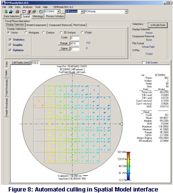
The Spatial interface shown in figure 8 displays the raw data for the BCD variable selected in the drop-down control at the top of the page. The user could also have selected a histogram, contour, 3D or general XY plot of the raw data.
Selecting the “Wafer” tab to the left of the screen will display data values as laid out on the substrate. Similarly, the “Field” tab will display data by site position on the exposure field.
Use the mouse to box-in any section of the graphic. The pop-up menu that appears will allow you to view the data points on a spreadsheet, cull the selected points or graph them using several graphic options.
OPC Radial Response
Pressing the “Cull-Radius” command button located on the upper left of the
graphic will plot the variable as a function of it’s radial location on the
wafer. This control is the first available control to allow separate OPC family
response plotting. Each family member will be plotted and a polynomial will be
fitted to the data. The user is asked to confirm the number of
“radial zones” to
include in this analysis and a polynomial order for the data fit prior to
generating the graphic. The radial analysis also generates two data
spreadsheets. The “RadialFit” spreadsheet presents the coefficients of the
fitted curve for each feature family. Similarly, the “RadialZones” spreadsheet,
shown in figure 9, reports the number of data points and their statistics for
each radial zone as specified. This report can then be saved along with its
graphic to any website by using the “File/SaveAs” menu in the excel spreadsheet.
OPC Characterization Prior to Culling
The following tools are used to characterize and determine the proper values to insert into the Range and Sigma culling fields. These tools can also be very useful to obtain a first evaluation of the relative response of each OPC feature across the raw data.
Data culling for soft metrology errors is performed by a comparison of the feature response to the median of the population. Culling is controlled for both raw and modeled analyses by entering values into the “Range” or “Sigma” fields shown in figure 8.
The Range control accepts a value that removes data that exceeds the specified deviation from the median of the population. In other words, a value of 2 nm entered in the Range field will removed any data point that extended +/- 2nm beyond the feature’s median value.
Similarly the Sigma field removes points based on their Standard Deviation from the feature-populations median. A Sigma of 1.24 entered here will therefore exclude all data points that exceed +/-(1.24 * Standard Deviation) of the population beyond the median.
Naturally the values to be entered into these fields are not intuitively obvious. A suite of analysis graphs can be generated to assist in your selection. These graphs also provide a rigorous analysis of the response and stability of each OPC family for the selected data variable. Start the analysis by pressing the “Range” command button located immediately to the left of the field, the multi-graph display shown in figure 10 will appear.
The analysis data can be viewed by using either the “Data/View” menu or the 2nd last button on the button bar. The last tab displays the median values calculated as a basis for these graphs. Six response graphs are presented:
Range
The number of data points (ordinate) residing within a given delta (abscissa) from the population median
Sigma
The number of data points (ordinate) residing within a given standard deviation (abscissa) from the population median
Delta from the median Distance of each point from the median
Population Mean
Mean of each family’s variable (ordinate) for the number of family members within the shown absolute delta from the median (abscissa). See figure 11
Population StDev
Standard Deviation of population
Population Range
Range of population members with the median delta
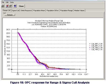
Figures 10 and 11 use a data set that has a full matrix of focus and dose variation. The four curves represent the response of two 90 nm OPC feature families nested in a 1:3 period. One curve is represented for Horizontal and Vertical tests of each family.
To use the “Range Cull” graph of figure 10 to determine the proper range-cull value for culling data examine the curve. This curve says that approximately 22 data points will be culled if a range value of 56.7 nm is used. The user can right-click on the graph to change the axis scale or to enter notes.
The curve of figure 10 can also be interpreted as a total of 176 data points of
each family are within 11.3 nm of the median, thereby showing the relative
response of each feature’s data to identical process variations. In this case we
see almost identical family response until approximately a deviation of 34 nm of
the median of the population. At the 34 nm point the bottom two curves continue
to show a tighter response suggesting that the “74E6” vertical and horizontal
features each respond better than the “38F7” design.

Population averages can also tell about the relative stability and response of the feature. The population-mean response graph of figure 11 shows that there is a fixed offset of roughly 2 nm between vertical and horizontal implementations of the feature and the “38F7” feature results in a larger feature size by about 5 nm across the focus-dose matrix.
Model Selection and Response
The classic method of evaluation of OPC Family response is to use a Process Window analysis. This method can be used in the Weir PW interface by pressing the “Process Window” button at the top of the screen of figure 12.
The Process Window method has many disadvantages. First it does not easily address the situation where there are multiple points on the field. The overlap of multiple feature windows is confusing particularly if there are features with multiple loading factors or orientations. The method is also inaccurate because the process-window control space is an expansion polynomial approximation of response that does not include the realities of whole-wafer process variation and a number of other aberration sources. Trying to fit a process window of this type to the varying exposure conditions found across each field is impractical and does not reveal the true response of each feature-design to process variation.
The Weir PW method fits a customized model to each exposure field on the wafer. If a scanner row or column model is selected, then every row or column will be fitted on every exposure field. This results of this method clearly delineate both the relative feature size supported by each OPC structure for a given focus and exposure as well that the structures response to the systematic variations experienced across the process range of exposures. Residuals show the level of random noise introduced by the metrology, process and exposure toolset.
Weir PW OPC model flow is:
-
Select the sub-population representing an OPC family
-
Optionally cull data points if Range or Sigma culling values are set
-
Model the wafer (if a wafer model is selected)
-
Record wafer fitted and residual data into workbook
-
-
Use the residuals of the wafer model to model every the field in the lot.
-
Record field fitted and residual data for each field
-
Repeat the sequence for the next family or exit modeling
-
Summarize results into the workbook and show response graphics
Typically a focus-exposure matrix analysis will not use the wafer model. In the example shown in figure 12 we selected the Full-Field model because the site-layout of the metrology does not lend itself to a row and column analysis.
Scanners are best modeled using the Row or Column models while steppers should use a Full-Field model. Row models optimize the analysis to find variations across the lens slit. Similarly the Column model selection optimizes the analysis for reticle-scan stage response.

OPC Modeled Results Reporting
The statistics shown to the right of the wafer in figure 12 first summarize the average set of field coefficients. The statistics below the coefficients represent the response of the systematic variation associated with the modeled coefficients. To see the response of any single or combination of field and/or wafer coefficients simply select the desired coefficients by checking the box next to them and remove checks from any coefficients not desired.
The “Validate” check box turns coefficient validity confirmation on (checked) or off (un-checked). When validation is not used, then all coefficients are used as returned by the surface-fit. When Validation is used then coefficients whose value is less then their uncertainty of determination are forced to zero and the model is adjusted to neglect the effects of this coefficient.
The Field Model selected will save two reports to the Weir Data Workbook. Naming of the spreadsheet takes the format of:
DataSheetType & Model & Variable Name
Example: “FieldModelSum_FullField_BCD”
The spreadsheets can be easily located from links in the “Index” spreadsheet and their function is:
|
Spreadsheet |
Function |
|
FieldModelSum_ |
A summary of every Row, Column or Field to which the model is fit sorted by family and exposure. Each coefficient and its uncertainty or estimation or standard error (“_SE”) is reported along with the Mean Square Error of the fit |
|
FieldResponse |
A report summarizing the fitted data. This report includes a header showing the data, data culling and range of exposure for the data.
|
Figure 13 shows a portion of the “FieldResponse_” report. The summary of the offset and residuals details the fields natural value for the feature-family and OPC design on the reticle. Statistics shown here display the contribution of the process, exposure and random variations to the variation of the feature. The objective of course is to select the structure design that will yield the desired size and exhibit the smallest variation in size when these process and exposure variations are encountered. Residual results include not only the process contributed variations but also the random errors caused by localized film variation and random response of the metrology and exposure tool. To see only the systematic influence of lens aberrations and exposure variation the systematic response of the feature must be views. These results are displayed in the next section of the spreadsheet table.

The summary of the systematic variations of the field show the systematic perturbations introduced by the process and exposure toolset. Theoretically this is the variation set that can be corrected if exposure is stabilized and exposure-tool aberrations are removed.
The systematic family-feature response to exposure focus and dose is best
understood with supporting graphics. The data is stored in a Microsoft Excel
Spreadsheet so it is relatively easy to create graphics on any data segment.
However the Weir PW software also creates a library of supporting graphics. This
library can be viewed in the multi-graph display that appears, the first graph
of which is shown in figure 14 for a set of “Top” or TCD feature data.
Family Response Graphics Library
The first 3 tabs of figure 13 summarize each family’s response with its associated error bars. The variable piston, in this case TCD or “Top Critical Dimension” features, supports error bars based on the standard deviation of the residuals to the piston or offset coefficient.
The Mean value curve is the field-average systematic error of all systematic modeled points in the fields as influenced throughout the exposure range. This plot supports error bars suggested by the uncertainty in the estimation of this mean value.
A large difference between the piston and mean curves of figure 14 indicates an exposure tool with significant across-field systematic errors or lens aberrations.
The next two tabs of the interface plot the Range and Standard Deviation of the systematic and residual components for each family. Again, these are two values that we desire to be at a minimum. The feature design that exhibits the minimum variation is therefore the optimum for this process.
The Weir PW OPC analysis can be extended to any number of families as shown in
figure 15. Figure 15 graphs the response of family features subjected to
differing loading conditions as 1:1, 1:2, and 1:3 spacing of nested features.
Both Vertical and Horizontal feature orientations were tested. The difference in
response for the four 90 nm targeted 1:1 dense packed features is clearly
visible and suggests that this exposure tool may not be suitable for 90 nm dense
lithography.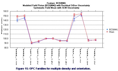
The two drop-down controls next to the “Refresh” button in figure 14 will change the available selection of graphs. The first control provides options that include an “All Dose” setting plus one selection for every unique dose and focus exposure in the data. Note that the data does not need to have multiple dose and focus exposure changes to see these graphics however the resulting entries in these two controls will change with the conditions of the input dataset. The graphs made available when these selections are changed adapt to the layout of the metrology data.
The second drop-down control lists the available OPC families just modeled.
Leaving the first control on “All Dose” and selecting a family name from the will provide a set of graphics showing the response of that family to focus for every unique dose as shown in Figure 16. This is of course the classic “Smile” plot.
In this example we can compare the response variation for the dense packed vertical and horizontal features. Figure 16 shows the Mean value, with error bars, of each dose curve. The mean values is plotted with error bars on these graphs report the Maximum and minimum systematic excursion of the data at each dose for the OPC feature. Unlike the standard “Smile” plot, you can also visualize the stability of the feature at each dose by plotting the “Range” and “StDev”; this is accomplished by selecting one of the last two tabs of the interface.

If
a single dose value is selected in the combo control, then the focus response of
each family is plotted against the focus value for each curve as shown in figure
17. This is an excellent tool for comparison of each feature’s response at a
given dose. As discussed previously, the Range and Standard Deviation can also
be shown.
The “clone” button located in the top button-bar will clone a copy of this interface. Cloning the interface provides a tool for graphic comparison of several response curves. For example, figure 18 shows a companion graphic of family response at 25 mj/cm2 and the onset of instability in the 1:1 feature for large focus offsets at 01 um. Quite interestingly, the 1:1 features appear to be more “Isofocal” in behavior near the optimum focus of -0.1 um than their less dense-packed counterparts.
The comparison of figures 17 & 18 implies that a larger depth of focus can be
achieved at 25 mj/cm2. Variation of systematic variation across the field also
drops radically for all features thereby suggesting a greater robustness of
performance at 25 mj/cm2.
However there is a rapid fall-off of control when
defocus moves above +0.05 um, perhaps rendering this exposure range impractical.
The following figures show some example graphics that can be obtained from the
interface.

This data is for a 90 nm target feature size. The spread shown in figure 19 for the 1:1 dense features across the fields at -0.05 um defocus (left figure) is greater than that at 0 um defocus. This illustrates that more than size is influenced by focus and dose uniformity.

Figure 20 similarly shows the response of each feature set with focus for Dose values of 24 and 25 mj/cm2. However, in this instance the Systematic Range of feature variation across the die is plotted as a function of defocus.
Notice how the 1:1 feature range of the left plot of figure 20 has a strong 2nd order dependence on optimum focus. We can also see her that the “34F7” dense packed features exhibit greater stability than their corresponding “24B2” design. Uniformity increases in the left graph at 25 mj/cm2 however we now see a large problem at the 0.1 um defocus values for the 38F7 design. This could be a “forbidden pitch” effect or may be an artifact of the processing.

Optical tools provide additional information beyond top and bottom feature width. Side-wall-angle (SWA) is an excellent tool for process design stability. In fact plotting the variation in Range and StDev across the systematic error field for the SWA is a stable method of finding the optimum focus for a tool as well as it’s exposure latitude. This is a greatly improved quantitative method of lens performance evaluation than the classic method of comparing several dozen SEM cross-section photographs.
Film uniformity is a another unexplored area of study. It’s a well-known fact that Anti-Reflective coating and photoresist thickness have a strong influence both the feature size and profile quality. Both films are monitored not only their thckness but also for uniformity. However both films have strong density changes that occur subject to the exposure intensity. Exposure intensity changes not with dose but with the coupling efficiency of the wavefront into the film. Therefore the thickness is sensitive to proper focus and optical aberrations across the exposure filed.
Figure 21 plots the plotted results of the full-field modeled data as a contour plot of photoresist thickness The classic signature of a focus-dose matrix exposure can be seen in the color changes of the plot. The same data organized by family is shown in the graph on the right side of the figure. The graph also shows that the 1:1 features result in less photoresist compaction while the 1:3 features show the strongest compaction.

Notice too the greater range of Photoresist variation across the field for the 1:3 features and the increased difference in results obtained from the mean field systematic value (blue curve) and their corresponding offset-coefficient (red) for the 1:3 features. This is caused by the switch-over in behavior of 1:3 pattern density features from that of a dense-packed structure to one that is beginning to behave as an isolated feature with greater sensitivity to lens aberrations.
Moving to Other Weir Interfaces
Weir program interfaces work interactively. You can move from Weir Main to any of the other five interfaces using the button-bar keys or the menu. Data is automatically transferred between interfaces. Any interface can load and, using the Weir Layout Library, configure exposure layouts for the arrays. Only the Weir Main interface can create Layout and Reticle Library Entries and Macros for the Weir Daily Monitor and DMA programs.
Interrupting Processing
-
The "ESC" key will interrupt any processing if it is held depressed.
-
Weir Reports can be saved to any website. To save the report, open it's spreadsheet in Excel and select the "File/SaveAs" menu. When the pop-up interface appears, select the "Web (htm,html)" format.
Graph Customization
-
Graphs are easily copied using the Edit Menu selections, the button bar and by boxing-in a section of any plot with the mouse.
-
To edit titles, rescale graphs, and add box-plots, trend-lines and fitted curves, right click on the graph and use the Graphic-Editor interface.
Spreadsheet Control
-
A "Spreadsheet" menu is located near the top right-hand corner of the Weir program interfaces. It will be listed as the name of the loaded Weir Workbook. The menu shown in figure 3 is using the name "KLA_SAMPLE.XLS".
-
Clicking on any spreadsheet menu will bring it to the forefront in the Excel Workbook.
-
Selecting the "Delete Worksheet" submenu will open an interface that will interactively allow multiple worksheets to be deleted from the workbook.
-
An "Index" worksheet positioned at the 3rd tab of the Weir Data workbook lists and links all of the worksheets created for data, reports and analysis summaries.
Automation
-
This entire analysis sequence can be automated to two-clicks of the mouse using Weir DM and Weir Automation Macros.
-
Weir DMA provides an external program portal for non-interactive analysis by Advance Process Control and Factory Automation programs.
TEA Systems
TEA Systems offers products to model films, photomasks, wafers, feature profile
s, process and lens data for characterization and setup of semiconductor design, simulators, tools and the process.
TEA Systems, a privately held corporation since 1988, specializes in advanced, intelligent modeling of the semiconductor process and toolset. Products from TEA allow the user to decouple process, tool and random perturbations for enhanced process setup & control.
TEA Systems products include:
Weir PSFM: Full-wafer/field/scan analysis tool for FOCUS derived from proprietary defocus sensitive features.
Weir PW: Reticle/Full-wafer/field/scan analysis for any metrology with advanced process window capabilities for both wafer and photomask control.
LithoWorks PEB: A tool to link and correlate profile, film and critical element control to thermal reactions such as PEB and ChillPlate
Weir DMA: Macro Automation interface for Weir PSFM and Weir PW for external program calling, automated data gathering or one-button analysis of commonly used sequences. Includes data trending and web interface.
* Excel is a trademark of Microsoft Corporation
ã Copyright 2006 TEA Systems Corporation, All rights reserved. Legal
TEA Systems
Corp. | Tel: +1 610 682 4146
65 Schlossburg St., Alburtis, PA USA